Data Layout and Its Notation#
Overview
A data layout maps a tensor’s logical indices to physical locations. This mapping determines not only whether the program reads the correct data, but also whether global-memory accesses coalesce, whether shared-memory accesses encounter bank conflicts, and whether a tile has the format required by a particular hardware unit.
The Shape-Stride model defines this mapping with a shape and a set of strides. Tiling uses the same model after splitting the original indices into more coordinates. Named axes extend physical locations to TMEM, warp lanes, and registers, while replication and offset represent data copies and fixed translations.
A swizzle rearranges shared-memory addresses without changing the logical shape of a tile. For a matching element width, alignment, and access pattern, an XOR swizzle can distribute accesses across memory banks and avoid bank conflicts.
Computations over the same values can differ in performance by an order of magnitude on the same GPU depending only on how those values are physically arranged in memory.
A tensor’s logical indices do not say where its bytes are actually stored. The hardware is highly sensitive to that placement. It determines whether loads from 32 lanes coalesce into one transaction or split across as many as 32, whether addresses land in different memory banks or collide and serialize, and whether a tile has a byte arrangement that a Tensor Core can read.
Machine learning programs usually describe a tensor by its logical shape. A data layout supplies
the missing physical information: it says where the element at logical index (i, j, …) resides,
whether in memory, in a register, or in another hardware storage space.
We begin with the Shape-Stride model and then extend the same notation to TMEM, register fragments, and multi-GPU layouts. The chapter ends with swizzling, which rearranges addresses to improve both row-wise and column-wise access to the same tile.
The Shape-Stride Model#
Before introducing GPU-specific layouts, we start with the Shape-Stride model. A shape gives the
size of each tensor dimension. The corresponding strides say how many physical elements to move
when a logical index increases by one along each dimension. We write the pair as
S[(shape) : (strides)]. The physical position of a logical index is the dot product of the index
and the strides. For example, a row-major 4×4 matrix is:
S[(4, 4) : (4, 1)]

addr(i, j) = i·4 + j·1
PyTorch and NumPy tensors already use this model: a flat storage buffer together with shape and
strides metadata that describes how to interpret the storage.
import torch

t = torch.arange(12).reshape(3, 4)
t.shape        # torch.Size([3, 4])
t.stride()     # (4, 1)        ← exactly S[(3, 4) : (4, 1)]
The underlying storage of t remains one-dimensional:
[0, 1, 2, 3, 4, 5, 6, 7, 8, 9, 10, 11]
Here, t uses S[(3, 4) : (4, 1)]: each row occupies four consecutive elements, and adjacent
columns are adjacent in storage. Many view-producing operations need only change the shape and
strides; they do not rearrange the elements. For a two-dimensional tensor, for example,
permute(1, 0) is equivalent to t.T:
tt = t.permute(1, 0)               # or t.T
tt.shape                           # torch.Size([4, 3])
tt.stride()                        # (1, 4)        ← strides swapped, no data moved
tt.untyped_storage().data_ptr() == t.untyped_storage().data_ptr()
                                   # True, still the same underlying storage
The transposed view uses S[(4, 3) : (1, 4)], so the address offset of tt[i, j] is
i·1 + j·4, exactly the location of t[j, i]. Calling view on a contiguous tensor, or calling
reshape when the existing layout is compatible, works the same way. NumPy follows the same model,
except that its .strides are measured in bytes rather than elements.
Tile Layout#
GPU kernels rarely process a full matrix at once. They usually divide it into smaller tiles. For
example, we can divide an 8×8 matrix into 2×4 tiles, store the tiles in row-major order, and also
store the elements within each tile in row-major order.
The figure below first shows this arrangement in the logical matrix and in physical memory.
Expressing Tiling as a Layout Function#
Describing the arrangement above requires both the tile’s position in the matrix and the element’s
position within that tile. Start with logical matrix coordinates (i, j) and flatten them according
to the original 8×8 shape:
x = i·8 + j
After dividing the matrix into 2×4 tiles, the row coordinate splits into four tile rows and two
rows within each tile. The column coordinate splits into two tile columns and four columns within
each tile. The shape used to decompose x is therefore:
(4, 2, 2, 4)
The layout unflattens x according to this shape:
(c0, c1, c2, c3) = unflatten(x; 4, 2, 2, 4)

c0 = x // 16
c1 = (x // 8) % 2
c2 = (x // 4) % 2
c3 = x % 4
Substituting x = i·8 + j gives:
c0 = i // 2    = tile_row
c1 = i % 2     = row_in_tile
c2 = j // 4    = tile_col
c3 = j % 4     = col_in_tile
We next map these four coordinates to a physical address. Each tile contains 2×4=8 elements, each
tile row contains two tiles, and each row within a tile contains four contiguous elements. Therefore:
The resulting layout is:
S[(4, 2, 2, 4) : (16, 4, 8, 1)]
Click any cell in the figure above to compare its tile coordinates and physical address with the unflattening process and \(f_D(x)\).
The General Layout Function#
The same calculation extends to a general Shape-Stride layout:
S[(e0, e1, ..., en-1) : (s0, s1, ..., sn-1)]
For a flat logical index \(x\), first unflatten it according to the shape:
Then take the dot product of those coordinates and the strides:
The shape determines how \(x\) is decomposed into coordinates, while the strides determine how those
coordinates map to a physical location. The tile layout above is the result of choosing shape
(4, 2, 2, 4) and strides (16, 4, 8, 1).
Named Axes: From Linear Addresses to Physical Coordinates#
The layouts above map every element to a linear memory address. Some GPU storage spaces, however, require more than one coordinate to identify a physical location. TMEM and register fragments are two direct examples.
The Two-Dimensional TMEM Address Space#
Blackwell TMEM is inherently two-dimensional. Each CTA has 128 lane rows and up to 512 32-bit columns. A position in TMEM therefore requires both a lane coordinate and a column coordinate.
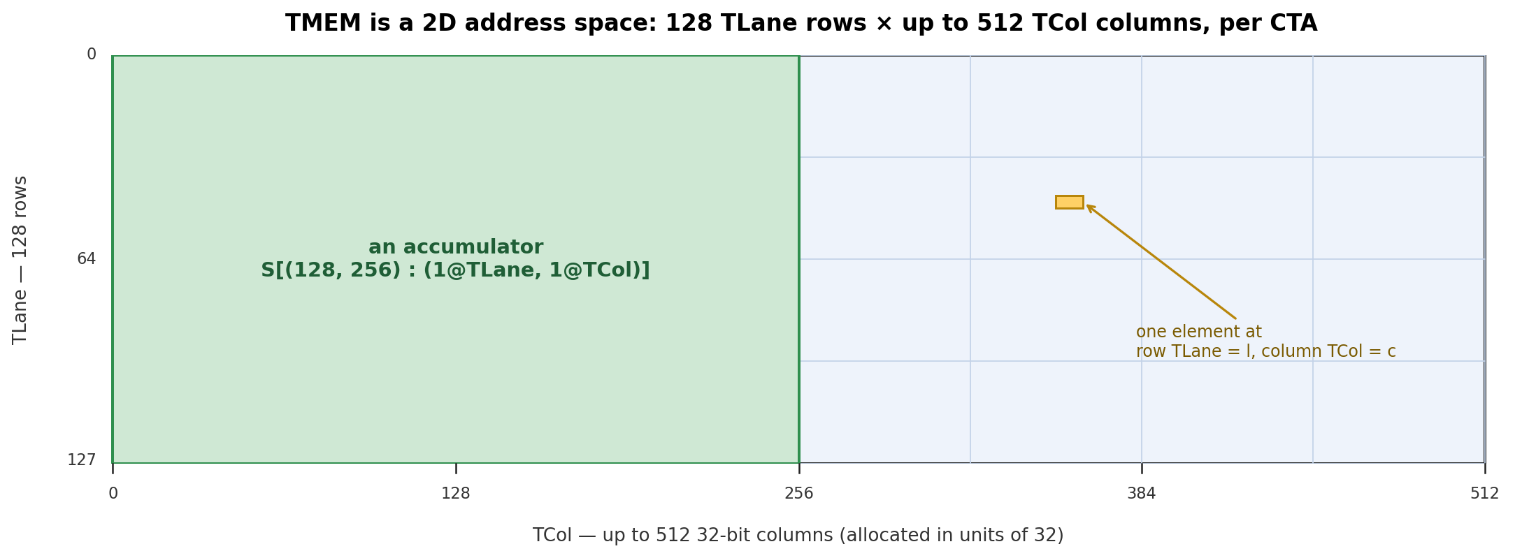
A single linear memory axis cannot distinguish these dimensions. We use @TLane and @TCol for the
TMEM lane and column axes. A 128×256 accumulator tile, for example, can be written as:
S[(128, 256) : (1@TLane, 1@TCol)]

(row, col) = unflatten(x; 128, 256)
f_D(x) = row@TLane + col@TCol
Here, \(f_D(x)\) no longer returns one integer address. It returns both TLane=row and TCol=col.
Ordinary linear memory, by contrast, has one address axis, @m. Making that tag explicit, a
row-major 8×16 memory tile is:
S[(8, 16) : (16@m, 1@m)]

(row, col) = unflatten(x; 8, 16)
f_D(x) = (row·16 + col)@m
Register Fragment#
Named axes also arise in the register fragments used by Tensor Cores. Consider an m8n8-style
fragment. Logically, it contains an 8×8 tile with 64 elements. Physically, those elements are
distributed across the 32 lanes of a warp, so each lane holds two fragment slots.
A lane ID alone is therefore not enough to identify an element. Its physical location has two parts: which lane owns it and which fragment slot it occupies within that lane. For this layout:
laneid = row·4 + col//2
reg    = col%2
The figure below shows how the 8×8 tile is distributed across warp lanes and registers.
Click cell 43 at row r5, column c3 in the Logical 8×8 Matrix on the left. The figure shows that
logical element (5, 3) is owned by lane 21 and occupies fragment slot 1 in that lane.
We represent these two coordinates with @laneid and @reg. The @laneid axis is the lane ID
within a warp; @reg is the fragment slot local to that lane. Here, @reg is a lane-local
coordinate in the layout. A specific instruction may still pack multiple low-precision elements
into one 32-bit hardware register.
The 8×8 tile can be written as:
S[(8, 4, 2) : (4@laneid, 1@laneid, 1@reg)]

(c0, c1, c2) = unflatten(x; 8, 4, 2)
             = (row, col//2, col%2)

f_D(x) = (c0·4 + c1)@laneid + c2@reg
Replication and Offset#
Broadcasting Scale Factors Across Warps in TMEM#
We begin with an example that occurs entirely within one kernel. Blackwell block-scaled MMA stores
scale factors in TMEM and makes them available to the four reading warps through a .warpx4
broadcast. As a result, one logical scale factor appears at four different TMEM lane positions.
Block-scaled MMA operates on low-precision inputs. It divides A and B along the K dimension into
scale blocks and associates one scale factor with each block to recover that block’s numerical
scale. If each scale block contains K_blk elements along K, the block containing element k is:
sfk = k // K_blk
Mathematically, block-scaled MMA is equivalent to scaling the A and B elements by their corresponding scale factors before performing the matrix multiply-accumulate:
A_real[m, k] = A_low[m, k] · SFA[m, k // K_blk]
B_real[k, n] = B_low[k, n] · SFB[n, k // K_blk]
D = C + A_real × B_real
SFA[m, sfk] is the scale factor for row m of A and K-scale block sfk; SFB[n, sfk] is the
corresponding factor for column n of B. The example below uses M = 128 and SF_K = 4, so the
logical shape of the A-side scale-factor tensor is 128×4.
Fix one value of sfk and consider the 128 elements SFA[m, sfk] for m = 0…127. They do not
occupy 128 distinct TMEM lanes. Instead, they are first packed as:
TLane  = m % 32
Mgroup = m // 32
TCol   = Mgroup
byte   = sfk

byte_offset = TCol·4 + byte
The ranges m = 0…31, 32…63, 64…95, and 96…127 reuse the same 32 TMEM lanes. For a fixed
sfk, the four Mgroup values map to TCols 0, 1, 2, and 3. Within each 32-bit TCol cell,
sfk = 0…3 selects one of its four byte sub-columns. The figure displays those cells as 16 byte
positions, with byte_offset = TCol·4 + sfk.
The .warpx4 broadcast then replicates this 32-lane layout along the TLane axis. For a base lane
l, the same value appears in lanes l, l+32, l+64, and l+96, while TCol remains unchanged.
Each of the four warps in the warpgroup can then read the value from its own 32-lane TMEM window.
Representing Multiple Physical Locations with Replication#
The function \(f_D(x)\) defined above returns only one location for logical element \(x\); it cannot
represent the additional copies created by .warpx4. We therefore append R[shape : strides] to
the base layout. For example, R[n : s@axis] introduces an independent replica coordinate
r = 0…n-1 and produces an offset of r·s@axis.
For the TMEM example, the four copies along the TLane axis are:
S[(32, …) : (1@TLane, …)] + R[4 : 32@TLane]
In R[4 : 32@TLane], r takes the values 0, 1, 2, and 3, producing TLane offsets of
0, 32, 64, and 96. The replication term does not add new logical data; it records the
physical locations of the copies.
The figure below shows both the packing rule and the four replicas along the TLane axis.
Click any scale factor to inspect its TMEM coordinate and its location in each of the four warp windows.
Replication and Offset in a GPU Mesh#
The same replication structure can describe a multi-GPU layout. A GPU mesh arranges multiple
GPUs along one or more logical device axes. A 2×2 GPU mesh contains four GPUs, each identified by
coordinates (@gpuid_x, @gpuid_y).
First define a base layout sharded along @gpuid_y:
base = S[(2, 4, 8) : (1@gpuid_y, 8@m, 1@m)]
Call the three logical coordinates (y, row, col). In the base layout, element (1, 2, 3) maps to:
gpuid_y = 1
m = 2·8 + 3 = 19
Adding replication gives:
base + R[2 : 1@gpuid_x]

Element (1, 2, 3) → devices {(0, 1), (1, 1)}, local offset = 19
The term R[2 : 1@gpuid_x] places the element at both gpuid_x = 0 and gpuid_x = 1. A fixed
offset behaves differently:
base + O[1@gpuid_x]

Element (1, 2, 3) → device (1, 1), local offset = 19
This offset translates the base location by one position along @gpuid_x; it does not create a
copy. The figure below compares these two cases with a fully sharded layout. Use the controls to
switch among fully sharded, shard + replica, and shard + offset.
Click any cell to see which devices hold the corresponding logical element.
Swizzle Layout#
The final layout in this chapter addresses bank conflicts in shared memory.
GPU shared memory is divided into memory banks. Each bank can be viewed as an independent channel that serves memory accesses. Accesses to different banks can proceed in parallel. If several lanes access different addresses in the same bank at the same time, however, the hardware must serve those accesses in separate batches, producing a bank conflict.
Tensor programs often access the same tile in more than one direction. Matrix code may read a contiguous row at one point and extract a column at another. A simple layout usually favors only one of these patterns. In a row-major tile, adjacent elements in a row have consecutive addresses and usually spread across different banks. Adjacent elements in a column are separated by a row stride. If that stride matches the bank-mapping period, accesses from several lanes can concentrate in the same bank. A column-major layout has the opposite tradeoff.
Swizzling mitigates this problem by changing the physical address arrangement while preserving the tile’s logical shape. A common technique XORs part of the row index into the column index so that the target access pattern spreads more evenly across the banks.
In the 8×8 example below, map logical coordinates (row, logical_col) as:
mapped_col    = logical_col XOR row
physical_addr = row·8 + mapped_col
XOR is bitwise exclusive OR. When reading logical column logical_col = 0, rows 0…7 produce
mapped_col = 0 XOR row = 0…7. Elements in one logical column therefore land in different physical
columns and, in turn, different banks.
Click a column index to compare the bank mapping of the plain row-major layout with the XOR swizzle. The former takes eight cycles; the latter takes one.
The figure above uses eight banks to illustrate the XOR rule. Real hardware applies the rule over a
larger repeating unit. We call each contiguous 16 B region a sector and represent it with one
colored block. In SWIZZLE_128B, each row of an atom contains eight sectors, for a total width of
128 B. At the common 4-byte bank granularity, that row spans 32 bank slots. The swizzle uses the row
coordinate to XOR-permute the eight sector positions.
A SWIZZLE_128B atom contains eight rows, so its total size is 8 × 128 B = 1024 B. Here,
128 B is the width of each atom row along the contiguous dimension, not the total atom size. The
atom is the smallest repeating block of the address permutation; larger tiles are formed by tiling
multiple atoms.
Each cell in the figure represents one 16 B sector. Step through the read cycles to see how XOR distributes a column access across different banks.
Other swizzle modes use the same hierarchy with a different row width. The atoms for
SWIZZLE_64B and SWIZZLE_32B are 8 × 64 B and 8 × 32 B, respectively.
The figure below compares these atoms directly and also includes a 16 B interleaved mode with no XOR swizzle.
Choose a swizzle format and data type to see the corresponding atom shape (8 × N B). Hover over a
cell to see where that element is remapped within the atom.
Which swizzle mode should you choose? A practical rule is to use the atom with the largest row width
that the tile can support. An atom whose row is N bytes wide requires the tile’s contiguous
dimension to be at least N bytes and preferably divisible by N.
For a row at least 128 bytes wide, or 64 float16 elements, SWIZZLE_128B is usually the preferred
choice. If the contiguous dimension is narrower than 128 bytes, use the largest supported
alternative: SWIZZLE_64B or SWIZZLE_32B.
For the fp16 access pattern shown above, SWIZZLE_128B makes both contiguous row reads and column
reads across eight rows conflict-free. This guarantee applies only when the element width, swizzle
mode, and access pattern match the hardware descriptor. Changing the element width, alignment, or
access pattern may reintroduce conflicts.
In practice, programmers do not compute swizzled addresses by hand. The full mapping can be viewed
as two steps: S[...] first maps a logical element to a linear memory address on @m, and the
swizzle then rearranges that address. Because the XOR permutation is not affine, the swizzle is not
part of the affine layout itself; it is a separate address transformation composed with that layout.
Every operation that accesses the same tile must use the same swizzle mode. The composed layout handles the actual address transformation. Different hardware units impose different swizzle requirements, and those requirements also change across GPU generations. The next chapter examines those constraints.