
The Evolution of Tensor Core Data Layouts#
Overview
On Ampere,
mma.syncreads A, B, and C from registers distributed across the threads in a warp, and D remains in registers.On Hopper,
wgmma.mma_asynccan read inputs directly from shared memory through matrix descriptors. The accumulator, however, remains distributed across per-thread registers.On Blackwell,
tcgen05.mmamoves the accumulator into TMEM. The scale factors used by block-scaled MMA also live in TMEM.
Mathematically, all three generations perform the same matrix multiply-accumulate:
A and B are the multiplicands, C is the incoming accumulator, and D is the result. The equation says nothing about where these matrices live or in what order the Tensor Core reads their elements.
This chapter fills in that missing physical picture. Tensor Core instructions interpret registers, shared memory addresses, and TMEM coordinates according to fixed hardware rules. Put one element in the wrong place, and the instruction will treat it as a different matrix element and produce the wrong result.
We will follow the data path through Ampere, Hopper, and Blackwell, asking the same three questions each time: Where does the MMA read its inputs? Where does it keep the accumulator? How does the kernel describe the layout expected by the instruction? We will use the notation introduced in Data Layout to write the concrete mappings.
Two Memory-Access Requirements to Keep in Mind#
Before looking at Tensor Core instructions, recall two other requirements that already constrain a GPU layout. Global memory addresses issued by a warp should combine into a small number of contiguous, aligned memory transactions. Shared memory addresses should spread across banks to avoid bank conflicts.
A practical Tensor Core layout must satisfy all three constraints: global memory accesses should coalesce, shared memory accesses should avoid conflicts, and every matrix element should occupy the position required by the MMA instruction. The first two were covered earlier. This chapter focuses on the third.
Ampere: Operands and Accumulators in Registers#
Start with Ampere. Its main Tensor Core interface is the mma.sync.aligned.m16n8k* family. mma.sync takes A, B, and C from registers and writes D back to registers.
A warp executes mma.sync collectively. PTX specifies how the A, B, and C/D tiles are distributed across the registers of its 32 threads. Each thread holds only part of a tile; that thread-local portion is its register fragment. Taken together, the 32 fragments represent the complete matrix tile.
Before issuing the MMA, an Ampere kernel will usually stage A and B in shared memory and then use ldmatrix to place the elements in the correct thread registers:
SMEM --ldmatrix--> registers
registers --mma.sync--> registers
registers --ordinary store--> SMEM or GMEM
At the moment mma.sync executes, only the register contents matter. The path above is the common high-performance route, but ordinary loads and register operations can prepare the same fragments.
A Concrete Fragment Mapping#
Consider mma.sync.aligned.m16n8k16. Let A be row-major and B be column-major, with fp16 or bf16 inputs and fp32 accumulation. The warp computes:
A thread’s lane ID determines which elements of A, B, C, and D it holds. We will begin with the C/D accumulator, where the pattern is easiest to see.
The figure below shows how the complete 16x8 C/D tile is distributed across 32 lanes. Each cell names the lane that holds that element. Matching fills connect the two rows assigned to one four-lane group, while the black borders mark lane 5’s four elements.
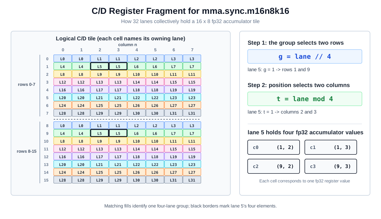
Read the figure in two steps:
The 32 lanes form eight groups of four. Group \(g\) owns rows \(g\) and \(g+8\).
The four lanes in that group split the eight columns. Position \(t\) owns columns \(2t\) and \(2t+1\) in both rows.
For lane ID \(l\), its group and its position within that group are:
Each lane therefore holds four fp32 accumulator values at:
The figure highlights lane 5. For this lane:
so it holds the following four C/D elements:
The A fragment uses the same \(g\) and \(t\), but its coordinates are \((m,k)\). Each lane holds eight fp16 or bf16 elements, with two adjacent elements packed into each 32-bit register:
At each of the two M coordinates, \(m=g\) and \(m=g+8\), the lane owns one adjacent pair in the lower half of K and another in the upper half.
The B fragment uses \((k,n)\) coordinates. Each lane holds four fp16 or bf16 elements, again with two elements packed into each 32-bit register:
For B, \(g\) determines the \(n\) coordinate, while \(t\) and the register number together determine \(k\).
We can now express the same mapping with the layout notation from the previous chapter. The first eight rows of C/D form an 8x8 local pattern:
S[(8, 4, 2) : (4@laneid, 1@laneid, 1@reg)]
The three coordinates are:
(row, column_pair, element_in_pair)
Adjacent columns form one column_pair, and element_in_pair selects one of the two columns. A matrix coordinate (row, col) therefore becomes:
(row, col // 2, col % 2)
The first two coordinates determine the lane ID, and the last determines the fragment slot within that lane:
lane_id = row * 4 + col // 2
slot    = col % 2
Return to the two elements (1,2) and (1,3) held by lane 5. Their atom coordinates are (1,1,0) and (1,1,1). Both map to lane 1*4+1=5; the final coordinate selects slot 0 or slot 1.
The complete C/D fragment contains two of these local patterns along M. The 8x8 atom is a convenient way to describe the layout; the hardware still executes one full mma.m16n8k16 instruction.
ldmatrix: Building a Fragment from Shared Memory#
We now know the register fragment expected by mma.sync. How do we move an A or B tile from shared memory into exactly those thread registers? Ampere provides ldmatrix for that job. Here are its .m8n8.b16 forms:
ldmatrix.sync.aligned.m8n8.x1.shared.b16
ldmatrix.sync.aligned.m8n8.x2.shared.b16
ldmatrix.sync.aligned.m8n8.x4.shared.b16
The whole warp executes the instruction together. The .x1, .x2, and .x4 variants load one, two, or four 8x8 matrices. For row r of matrix m, lane m*8+r supplies the row’s base address. Thus .x1 takes addresses from lanes 0-7, .x2 from lanes 0-15, and .x4 from all 32 lanes.
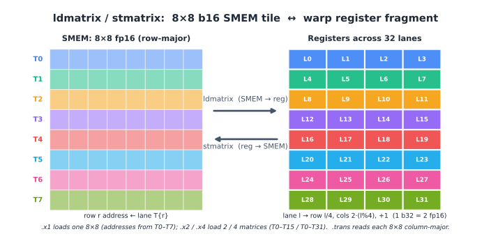
The figure below shows .x1. Threads T0-T7 on the left supply the eight row addresses, but supplying an address and receiving data are separate roles: the 64 loaded elements are distributed across all 32 threads. Lane \(l\) receives:
row  = l // 4
cols = 2 * (l % 4), 2 * (l % 4) + 1
For example, the eight elements in row 0 go to lanes 0-3. Lane 0 receives columns 0-1, lane 1 receives columns 2-3, and so on. The two fp16 elements received by each lane are packed into one 32-bit register. The left side of the figure shows which lanes supply addresses; the right side shows which lanes hold the data after the load. The reverse arrow is stmatrix, introduced on Hopper (sm_90) to store a register fragment back to shared memory.
The optional .trans qualifier loads each 8x8 matrix in column-major format. A kernel can also build a fragment with ordinary loads and register operations, but then it must implement this cross-lane distribution itself.
Writing Back and Swizzling Shared Memory#
After mma.sync, C/D remains a register fragment. On Ampere, the epilogue normally uses ordinary per-thread stores to write the result to shared memory or global memory, with warp shuffles or local rearrangement when needed.
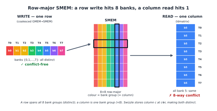
The input path presents another layout problem: ordinary stores favor consecutive elements along a row, while ldmatrix later reads across rows. One shared-memory layout has to serve both patterns. For an (8,64) float16 tile, each row occupies exactly 128 bytes. With the usual 4-byte bank granularity, eight elements in a fixed column can all map to the same bank because the row stride is 128 bytes, producing an eight-way conflict.
Ampere kernels commonly change the physical shared-memory placement with hand-written XOR address calculations. This preserves efficient contiguous row accesses while spreading cross-row reads across banks. The previous chapter developed this idea in detail; the figure below shows the contrast again.
Hopper: Reading Directly from Shared Memory#
WGMMA: Four Warps Cooperate on One MMA#
Hopper widens the MMA from one warp to one warpgroup. A warpgroup consists of four consecutive warps, or 128 threads, that execute wgmma.mma_async together.
The more important change is the input path. B comes from shared memory through a matrix descriptor. A may also come from shared memory, or it may come from registers. These two forms are commonly called SS and RS:
SS: A from SMEM, B from SMEM -> wgmma -> register accumulator
RS: A from registers, B from SMEM -> wgmma -> register accumulator
For a shared-memory operand, the kernel no longer uses ldmatrix to build an A or B register fragment. WGMMA reads the data directly, but it still needs to know where the matrix begins, how far to move between data groups, and which shared-memory swizzle is in use. A matrix descriptor carries that information.
How a Matrix Descriptor Locates a Tile#
A matrix descriptor is a 64-bit value held in a register. Think of it as an addressing recipe for WGMMA: the matrix data remains in shared memory, while the descriptor tells the instruction how to find and traverse the tile.
Field |
What it describes |
|---|---|
|
The beginning of the matrix in shared memory |
|
The byte offset used to reach the next group along the leading dimension |
|
The byte offset used to reach the next group along the stride dimension |
|
The matrix start within the repeating swizzle pattern |
|
No swizzle, or 32-byte, 64-byte, or 128-byte swizzling |
WGMMA starts at matrix start address, then uses ldo and sdo to reach later data groups. All three address fields are encoded in units of 16 bytes. The major mode and swizzle mode determine which matrix direction corresponds to the leading and stride dimensions.
For a swizzled K-major layout, ldo uses the fixed encoding 1, while sdo gives the byte offset from one eight-row group to the next. The swizzle mode determines the atom shape and the XOR permutation within each atom. matrix base offset locates the matrix start within that repeating pattern; it is zero when the start is aligned to the pattern boundary.
The figure makes this concrete. The A operand uses a K-major layout with 128-byte swizzling. K runs horizontally, M runs vertically, and each colored block is an atom with eight 128-byte rows. The black dot at the upper left marks start_address. K follows the fixed atom layout, so ldo is encoded as 1. Moving down by eight rows uses sdo to reach the next group. Once the descriptor identifies the target atom, the swizzle mode determines the byte position within it.
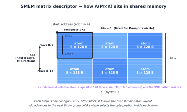
This is why the descriptor must agree with the bytes in shared memory. If TMA writes a tile with 128-byte swizzling, the WGMMA descriptor must interpret the tile with the same 128-byte swizzle. TMA and WGMMA use separate descriptors for separate instructions, but both must describe the same physical arrangement.
Accumulators Remain in Registers#
WGMMA reads shared-memory inputs directly, but C/D is still distributed across the registers of the threads in the warpgroup. The epilogue consumes these register fragments. The instruction shape and accumulation type determine how many accumulator values each thread holds.
A Hopper kernel therefore works with two layout representations at once. Matrix descriptors describe A and B in shared memory; per-thread register fragments describe register-sourced A and the C/D accumulator. B always uses the shared-memory path, while A may use either path.
Blackwell: Moving Accumulators into TMEM#
Accumulators in TMEM#
Blackwell keeps Hopper’s descriptor-based input path. tcgen05.mma uses descriptors to find A and B in shared memory and read them in the required layout. Some modes also allow A to come from TMEM.
The major change is where the accumulator lives. Hopper keeps C/D in the registers of the participating threads; Blackwell places it in Tensor Memory, or TMEM. When the epilogue needs the result, tcgen05.ld loads the data into registers:
A/B in SMEM --tcgen05.mma--> C/D in TMEM
C/D in TMEM --tcgen05.ld--> register fragment --store--> GMEM
tcgen05.mma executes asynchronously. After issuing the instruction, the kernel must wait for the MMA to complete before the epilogue reads the result with tcgen05.ld. The load is asynchronous as well, so the epilogue must execute tcgen05.wait::ld before using the destination registers. The write and read layouts have to match: whatever TMEM lane and column coordinates receive an element from tcgen05.mma must provide that element to the corresponding thread register during tcgen05.ld.
Scale Factors for Block-Scaled MMA#
The Broadcasting Scale Factors Across Warps in TMEM section in the previous chapter used M=128 and SFK=4 to derive the TMEM packing and .warpx4 replication of scale factors. We now pick up that data path where it left off: how do those values enter TMEM, and how does the MMA select the bytes needed for one operation?
Block-scaled MMA uses two scale-factor matrices:
SFA(M, SFK)
SFB(N, SFK)
SFA[m,sfk] scales row m of A for K-scale block sfk. SFB[n,sfk] does the same for column n of B. We keep the logical index order introduced in the previous chapter; PTX tables write the same B-side matrix as SFB[sfk,n], with shape SFB_M x N.
TMA usually loads A and B into shared memory, where the MMA reads them directly. Scale factors need to reach TMEM, while TMA stops at shared memory, so they take one additional step through tcgen05.cp:
A, B:     GMEM --TMA--> SMEM --tcgen05.mma--> Tensor Core
SFA, SFB: GMEM --TMA--> SMEM --tcgen05.cp--> TMEM --tcgen05.mma--> Tensor Core
How tcgen05.cp Writes TMEM#
Recall the complete layout derived in the previous chapter:
S[(4, 32, 4) : (4@TCol, 1@TLane, 1@TCol)]
+ R[4 : 32@TLane]
S[...] maps (Mgroup, lane, sfk) to byte positions in TMEM. In a typed TIRx layout, @TCol strides are measured in buffer elements. A scale factor is 8 bits here, so the logical TCol position is 4*Mgroup+sfk; every four consecutive positions pack into one 32-bit hardware TCol cell. Equivalently, hardware_TCol=(4*Mgroup+sfk)//4 and byte_in_word=(4*Mgroup+sfk)%4.
R[...] adds four replicas along TLane. The .32x128b.warpx4 form of tcgen05.cp creates this layout by multicasting the same base tile into four 32-lane warp windows.
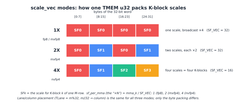
Word-Level Replication for scale_vec#
Once the values are in TMEM, one more layout rule applies inside each 32-bit TMEM word. scale_vec determines whether each row of SFA, or each column of SFB, contains one, two, or four logical scales. Shorter scale vectors repeat within the four-byte word:
scale_vec::1X: [SF0, SF0, SF0, SF0]
scale_vec::2X: [SF0, SF1, SF0, SF1]
scale_vec::4X: [SF0, SF1, SF2, SF3]
SFA_ID or SFB_ID tells the MMA which copy to read. With 1X, the byte offset may be 0, 1, 2, or 3. With 2X, offset 0 selects the low half-word and offset 2 selects the high half-word. With 4X, all four bytes are used, so the ID must be 0.
This repetition within a word is separate from R[4 : 32@TLane]: the former repeats bytes inside a 32-bit word, while the latter replicates data across four TMEM lane windows. A scale’s mathematical reuse across every K element in its block is a third, separate idea.
Per-Thread Register Fragments Across Generations#
Across all three generations, matrix data passes through register fragments distributed across threads. The exact fragment shape and mapping depend on the instruction.
On Ampere, ldmatrix loads shared-memory data and builds the register fragment consumed by mma.sync.
On Hopper, wgmma writes its accumulator into register fragments for the epilogue.
On Blackwell, the accumulator stays in TMEM during the compute phase. Before the epilogue begins, tcgen05.ld loads the result into register fragments.
The role of the register fragment therefore changes across generations. Ampere and Hopper use it to hold the accumulator during computation. Blackwell uses it mainly at the boundary between TMEM and the epilogue. The m8n8-style atom shown earlier is one common example; tcgen05.ld and tcgen05.st also provide several other data-movement shapes.
Comparing the Three Data Paths#
Architecture |
Main MMA instruction |
Main source of A/B |
Accumulator location |
How the shared-memory layout is expressed |
|---|---|---|---|---|
Ampere |
|
Registers |
Registers |
The kernel usually computes addresses and swizzles explicitly |
Hopper |
|
A may come from registers or SMEM; B comes from SMEM |
Registers |
A matrix descriptor records strides and the swizzle mode |
Blackwell |
|
Primarily SMEM; some modes take A from TMEM |
TMEM |
Descriptors cover SMEM inputs; TMEM layouts describe accumulators and scale factors |
Side by side, the progression is clear. Ampere arranges inputs as per-lane register fragments. Hopper lets the Tensor Core consume shared memory directly through descriptors. Blackwell then moves the accumulator and scale factors into TMEM.
When implementing a kernel, trace the data flow one step at a time: the layout written by one instruction must be the layout read by the next. If any step interprets the physical arrangement differently, the Tensor Core may consume the wrong elements. Even when the result remains correct, a mismatched access pattern can still waste performance.